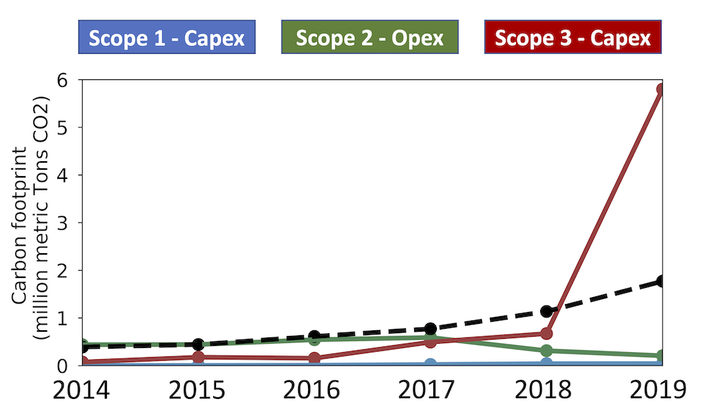
Research communities in computer systems should worry about capex carbon emissions. Capex or embodied carbon accounts for the carbon manufacturers produce when building a machine. It’s in contrast to opex carbon, which counts the emissions we incur to use a machine, i.e., from the electricity we feed into a datacenter or a smartphone’s charging port. In a way, systems researchers are already all experts on opex carbon: we worship at the temple of computational efficiency, and making machines faster almost always means getting more work done per joule of energy. But researchers have recently suggested that, over the lifetime of a computer system, its capex carbon can outstrip—perhaps dramatically—its opex emissions.
If capex carbon is the real problem in computing’s climate impact, systems researchers should worry because our favorite tools are a poor fit for the job. It does not suffice to design new and better computers that work more efficiently than the old computers, as we usually do; we instead need to figure out how to use the same old hardware for longer. Reuse and longevity are the key metrics for climate-aware computing.
Meanwhile, a technology trend is promising a different kind of reuse: multi-chip modules (MCMs) replace one big chip with a network of separately manufactured chiplets. Chiplets are suddenly everywhere: AMD’s latest Threadripper parts have 9 dies, and Intel’s Ponte Vecchio GPU consists of 47 chiplets. One selling point for the chiplet revolution is the cost-saving advantage of design reuse: you can tape out one chiplet and use it across several MCM products. Four of seven chiplets in AWS’s Graviton3 MCM, for example, are DDR5 memory controllers. It’s not hard to imagine that these DDR5 chiplets will still be useful for next year’s AWS server product, so AWS can amortize the cost of building that chiplet across multiple generations.
Reusing chiplets saves money, but it does not save capex carbon. Every MCM still consists of brand-new silicon, with all the concomitant manufacturing emissions, just like a monolithic chip.
What if there were a way to literally reuse chiplets? To recover chiplets from old and obsolete MCMs that could still be useful as a building block for new products?
Silicon Recycling
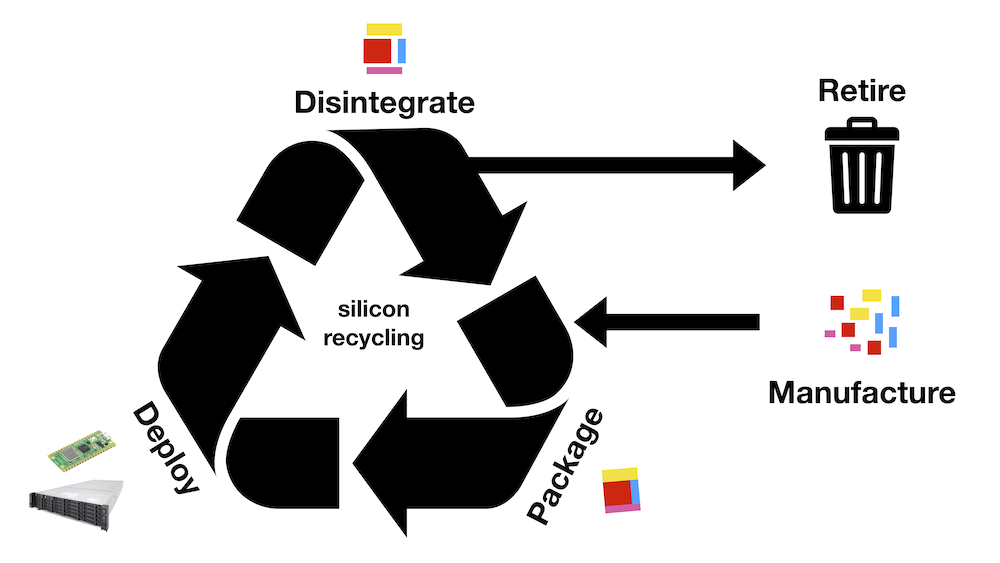
We envision silicon recycling: an imaginary world where we make new MCMs by harvesting chiplets from old computers and remixing them in new ways. Silicon recycling is the general principle of design for active disassembly applied to integrated circuits. In the same way a couch or a toaster could be built with debondable adhesives to make recycling easier at the end of its life, the idea is to build MCMs with a debondable process.
In the real world, MCM packaging uses a bonding process to attach chiplets to a silicon interposer. I like to imagine the world’s tiniest soldering iron (at, say, a 10 μm pitch) attaching the bumps on each chiplet to the corresponding pad on the interposer. In our imaginary world of silicon recycling, the idea is to (somehow) make this bonding process reversible. We build the MCM in the same way, but we design the bonding process that makes it possible to undo the tiny, metaphorical soldering job. By applying heat, lasers, some magical solvent, or a combination of the three, the chiplets break free from the interposer—and both are undamaged, ready to be bonded again in a new product.
In a hypothetical world with silicon recycling, when you upgrade your phone and send your old one off for recycling, the recycler doesn’t just recover the precious metals from the case, PCBs, and screen. They also take the MCM at the heart of the machine, debond all its chiplets, and put them up for sale on a marketplace for second-hand silicon. Your smartphone’s chiplets may go into a next-generation smartphone, coupled with some brand-new chiplets that differentiate it, or they may go downmarket into a camera or a microwave.
Reversible Packaging is a Fantasy (For Now)
The problem with this vision is that it is science fiction. In the real world, bonding is irreversible—there is no way to safely disassemble an MCM and recover working chiplets.
I am very far from an expert on bonding and packaging—I base this conclusion only on a reasonably thorough literature search that turned up no indication that anyone is even working on reversible bonding for MCMs. The closest thing appears to be temporary bonding technologies, which which are useful during the manufacturing process. For example, some technologies temporarily bond chiplets to silicon or glass carriers while processing them; then, IR lasers debond the silicon (avoiding any mechanical force) before packaging. The final MCM uses a permanent bond.
On the other hand, I did not find evidence that reversible bonding is infeasible in principle. The vacuum in the literature seems to indicate that no one is trying, perhaps because the idea is just too ridiculous.
Research Directions in Computer Systems
Reversible packaging is a problem of materials and technology—not something that can be solved by systems-level research: architecture, programming languages, operating systems, and the like. But the consequences of silicon recycling technology would be systems problems. Even though it is not yet practical, we can already imagine the systems research that silicon recycling would entail:
Carbon-Aware Architectural Disaggregation
The silicon recycling vision needs architecture research that explores how to build MCMs that maximize their potential for reuse. As in brick and mortar architecture, the idea is to take your favorite monolithic processor design and disaggregate it into little chiplet-sized pieces. Disaggregated architectures need to balance two goals: bigger chiplets can better mitigate the costs of inter-chiplet communication, while finer-grained chiplets are more reusable. An ALU chiplet is more likely to be useful in future designs, for example, than a chiplet that bundles together a particular processor’s needs for arithmetic, registers, address calculation, pipeline bypassing, and branch prediction. But a single ALU is probably too tiny to be practical as a standalone chiplet. This kind of disaggregated architecture research needs to start with a prior assumption about what other, future architectures will look like. Today’s designs can then use this prior to maximize the likelihood that their components will be useful in tomorrow’s designs.
Tools for Design from Spare Parts
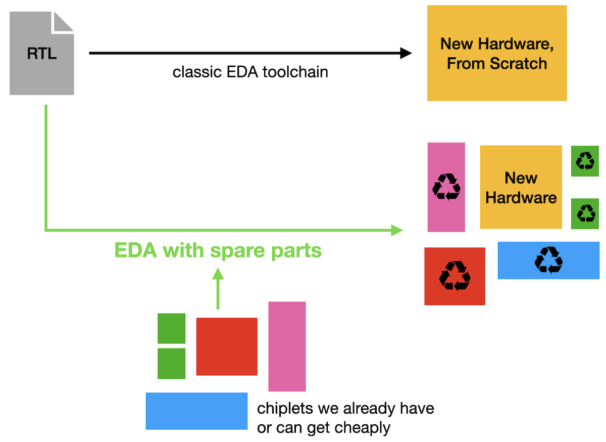
Today’s design tools all produce hardware “from scratch.” To wildly oversimplify, you feed in your HDL code and the toolchain produces a physical design ready to tape out. To enable silicon recycling, we will need tools that can synthesize hardware made from an inventory of “spare parts”: chiplets we have on hand or think we can easily buy. In spare-parts synthesis, the designer feeds in (alongside their HDL code) a list of descriptions of all that second-hand hardware; the toolchain’s job is to produce a design for a complete MCM that maximizes the use of those repurposed chiplets. The tools will surely still need to generate some new, project-specific hardware, but the goal is to make this fresh silicon a minority of the overall area.
Physically Reconfigurable Hardware
Today’s reconfigurable hardware—FPGAs and CGRAs—give you a toolbox of components that you can hook up however you like. But the mixture of components in each toolbox is fixed. If you buy an FPGA from AMD, for example, the FPGA comes with a fixed ratio of basic logic elements (LUTs) to memories (BRAMs) to arithmetic units (DSPs). With silicon recycling, we could make physically reconfigurable hardware: where you start with an assortment of LUT chiplets, BRAM chiplets, and DSP chiplets and mix them in the proportion and arrangement that your application domain demands. Once you have crafted your custom FPGA MCM, you then configure and reconfigure it as many times as you need to implement your application as it evolves. Physically reconfigurable FPGAs need a kind of two-level compiler: they need to jointly produce (1) a physical configuration of chiplets into an FPGA, and (2) a logical configuration of the FPGA into your design. This kind of compiler needs to be aware that physical reconfiguration is expensive and logical reconfiguration is cheap, so the former should admit as much flexibility in the latter as possible while still optimizing for efficiency.
A Call to Action
I confess that I do not know how feasible reversible MCM packaging is. It may be a technical impossibility. But it seems equally likely that it’s the victim of a chicken-and-egg problem: it doesn’t exist, so no one has done the research on how to exploit it for silicon recycling, so there is no pressure to develop the technology, so it doesn’t exist.
Given the urgency of mitigating computing’s capex carbon footprint, we should break this incentive deadlock. Systems researchers should rush ahead and do the work to understand how to design for reusability and how to exploit second-hand chiplets. By demonstrating the systems-level potential for silicon recycling, we can create the incentive to develop the technology that will make it possible.