Project 2 - Fully Pipelined Mips
CS3410 Library Components Guide
Using MIPS RAM as byte addressed and little endian RAM
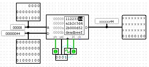
Here is a screenshot as I am writing the byte value 0x44 into byte address 32. Since the RAM is word addressed, this byte gets written to one of the four bytes at word address 32/4 = 8; you can see the A input to the RAM is 8. Since I want little-endian behavior, address 32 corresponds to the little end of the word (address 35 would be the big end of the same word, where 0x11 is stored); you can see the selector input is set to activate only the little end of the word. I am also reading at the same time, so you can see the 0x44 being read out on the litle end of the D output. If I were to activate all of the selectors, the RAM would output 0x11223344, which is the word stored at word address 8, i.e. byte address 4 * 8 = 32, which contains bytes 32 through 35.
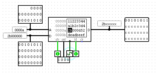
Here is another screenshot as I am writing the byte value 0x2b into byte address 43. Since the ram is word addressed, this byte gets written to one of the bytes at word address 43/4 = 10; you can see the A input to the RAM is 0xa = 10. Since I want little-endian behavior, address 43 corresponds to the big end of the word (address 40 would be the little end of the same word, where 0x52 is stored); you can see the selector input is set to activate only the big end of the word. I am also reading at the same time, so you can see the 0x2b being read out on the big end of the D output. If I were to activate all of the selectors, the RAM would output 0x2b000d52, which is the word stored at word address 0xa = 10, i.e. byte address 4 * 10 = 40, which contains bytes 40 through 43.
For writing byte 0xbb, depending on the address, I might want to put it at the big end, little end, or somewhere in the middle. Similarly for reading a byte, depending on the address, I might want to grab the bytes from the big end, little end, or somewhere in the middle. Hint: For writing, just direct the desired byte to all four positions then activate writing for just the one you want. For reading, you will need to select between the four possible positions where the byte might appear on the RAM's D output.
On the other hand, reading and writing whole words is trivial. The RAM is 32 bits wide, so just send the whole 32-bits to the memory, and read the whole 32-bits back to the CPU. You could try to be clever by swapping the order of each word's four bytes when writing to RAM, and un-swapping them when reading from RAM. This, however, would be entirely pointless. Can you tell why? Try it to see if it makes it any easier to read and write bytes.
cs3410 Component Library Guide
The "CS3410 Components" library will only appear if you are using the most recent version of Logisim, downloaded from the course website. Please ensure that you are using the correct version. If so, you should have a folder in your sidebar containing the following components:
|
MIPS RAM. This component is identical to Logisim's regular 32-bit wide, word-addressed RAM component, except the single-bit sel input is replaced by a 4-bit input to selectively enable or disable access to individual bytes within a 32-bit word. For instance, if the memory contains the word 0xAABBCCDD at the current address, then sel=0011 will access only the least significant halfword (0xCCDD), and sel=1000 will access only the most significant byte (0xAA). This component does not have a defined endianness since it is word addressed. Byte addressed memory (either little-endian or big-endian) can be emulated: to access byte-address 4 (the fifth byte in memory) in little-endian mode, one would set a=1 (second word) and sel=0001 (least significant byte); to access byte-address 4 (the fifth byte in memory) in big-endian mode, one would set a=1 (second word) and sel=1000 (most significant byte). |  |
Register File. A 32-bit wide by 32-registers deep register file. Register |
 |
||||||||||||||||||||||||||||||||||||||||
|
MIPS Program ROM. A 32-bit wide byte-addressed ROM, with built-in MIPS assembler. Use the attributes
panel to load a MIPS assembly file into the ROM. The |
 |
||||||||||||||||||||||||||||||||||||||||||
|
MIPS ALU. Computes a result as follows:
|
 |
||||||||||||||||||||||||||||||||||||||||||
|
Incrementer. An adjustable-width incrementer. Takes its input |
|
||||||||||||||||||||||||||||||||||||||||||
|
LCD Video. If |
 |