Project 1 - ALU Design
CS 3410 Spring 2019
Project Due: February 15, 2019 at 11:59:00pm
Please submit all required documents to CMS.
You must work ALONE for this and all other individual projects.
Failure to adhere to this rule will result in an Academic Integrity Violation.
You will only be able to work in groups for designated group projects. Updates to this assignment will be
posted on the course web page.
Overview
In the first four projects you will design a subset of the RISC32 architecture in Logisim, a software logic
simulator. The goal of these projects is to move you from designing small special-purpose circuits to
building complex, general-purpose CPUs. By the end of the third project, you will have designed a
32-bit pipelined RISC CPU. For these assignments, we will ignore more advanced features, including the RISC
coprocessor instructions and traps/exceptions.
In this project, you will design a RISC ALU (arithmetic and logic unit) which performs all of the core
computations dictated by the assembly language. You have already seen pieces of the ALU, such as a 32-bit
adder circuit, in class. You can also consult section A.5 in your textbook.
We will be using Logisim, a free hardware design and circuit simulation tool. Logisim comes with libraries
containing basic gates, memory chips, multiplexers and decoders, and other simple components. In later
assignments, you will use many of these components to build your final CPU.
However, for this
assignment you may only use the following Logisim elements:
- Anything in the Wiring except for the resistor, constant, power, ground and transistor elements.
- Anything in the Base folder (wires, text, etc.)
- Anything in the Gates folder except for the even parity, odd parity, and controlled buffer
elements
- Anything in the Plexers folder
**Important - Use this guideline for
designing your circuits to avoid losing points!**
Academic Integrity.
As one of the most widely studied architectures, RISC has a wealth of information available on the web and in
textbooks. You may consult any RISC documentation available to you in order to learn about the instruction
set, what each instruction does, how an ALU works, etc. However, we expect your design to be entirely your
own, and your submission should cite any significant sources of information you used. If you are unsure if it
is okay to borrow from some other source, just ask the TAs. If you are hesitant to ask the TAs or to cite the
source, then it is probably not okay. Plagiarism in any form will not be tolerated. It is also your
responsibility to make sure your sources match the material we describe here.
All of the following should be subcircuits in a single Logisim circuit file. To get you started we've
provided an ALU_template.circ file
with all the appropriate inputs and outputs specified.
What to Submit
- A single Logisim project file containing your ALU and all needed subcomponents. Please ensure that
your circuit has no external dependencies!
-
We will use Logisim's test vector function to test your circuits. In order for it to work correctly,
you must ensure that the Logisim circuits containing your solutions are named precisely "LeftShift32",
"Add32", and "ALU32", and the inputs/outputs are named "A", "B", "Op", "Sa", "C", and "V". Use those
inputs/outputs, not your own!
-
A design document that details the implementation of your circuit.
-
A README.txt with your name, NetID, critical path, and gate count.
-
Three text files containing your test vectors, one for each of the Left Shifter, Adder, and ALU circuits.
Circuit 1: LeftShift32
You implemented this circuit in Lab 2, but in case your design had issues, we've replicated the
specification below. The completed ALU you submit will need this piece to work.
| LeftShift32: |
C = (B << Sa) | carrybits |
| Inputs: |
B[32], Sa[5], Cin |
| Outputs: |
C[32] |
The output C is computed by shifting B to the left Sa bits, and
filling the vacated bits on the right with carrybits, which is just Sa copies of
Cin. The shift amount Sa can be anything from 0 to 31, encoded as an unsigned
integer.
Note: Some inputs and outputs are busses (as noted by the bus width in brackets); the rest are 1-bit wide.
One way to implement such a shifter is to perform the shift as a series of stages: the first stage shifts
either 0 or 16 bits, the second stage either 0 or 8 bits, the third stage either 0 or 4 bits, and so on. By
enabling different combinations of stages, the circuit can shift any desired amount. Hint: Shifting a
value on a 32-bit bus by a constant amount, either left or right, is simply a matter of adding, removing, and
renaming the wires on the bus, and so requires no gates at all.
Circuit 2: Add32
| Add32: |
C = A + B + Cin; V = overflow |
| Inputs: |
A[32], B[32], Cin |
| Outputs: |
C[32], V |
The output C is computed by adding A, B, and Cin. A,
B, and C are signed two's complement numbers. If overflow occurs, the output
V should be asserted. In such cases, the output C should correspond to the value
computed if all overflow errors are ignored. Hint: Use subcomponents to make wiring easier by building
a 1-bit adder, then a 2-bit adder, then a 4-bit adder, and so on up to 32-bits.
Signed vs. Unsigned Adders
There actually isn't a huge difference between signed and unsigned adders. In fact the only difference
between the two is the way that overflow is calculated. Below is a 4-bit unsigned adder, like the one you did
in Lab 1...
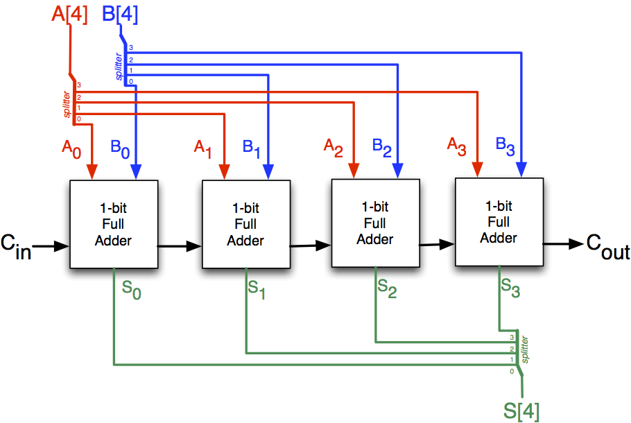
...and here is everything you need to add to it so it can behave like a 4-bit two's complement signed adder.
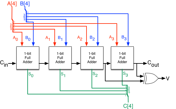
Not much at all! Also, note that the one-bit adder subcircuits in both the signed and unsigned 4-bit adders are identical (the
one-bit adders are all unsigned adders). Use this distinction when building your 32-bit signed adder.
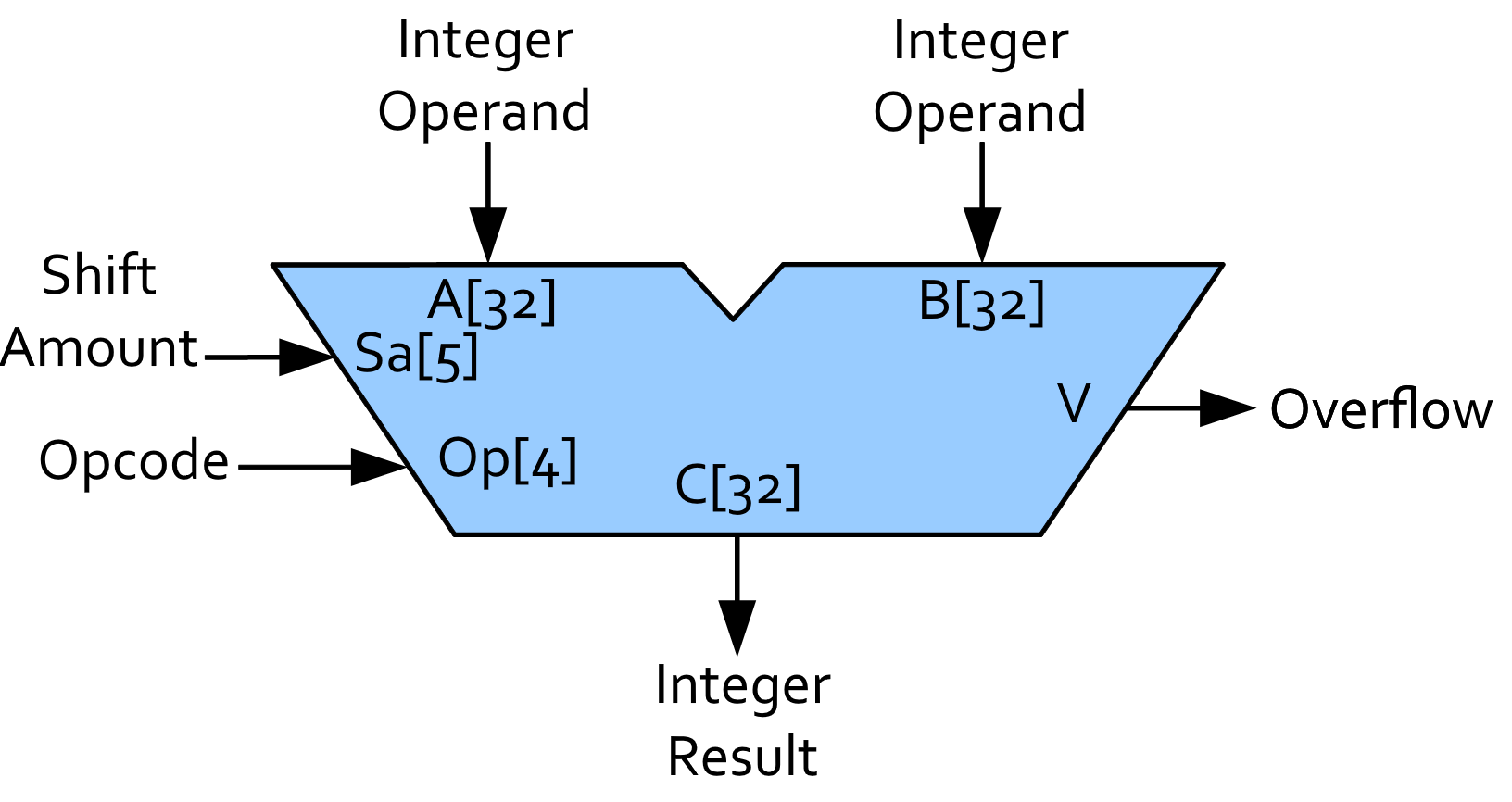
Circuit 3: ALU32
| ALU32: |
(C, V) = fOp(A, B, Sa) |
| Inputs: |
A[32], B[32], Op[4], Sa[5] |
| Outputs: |
C[32], V |
The C and V outputs are computed according the value of the Op input
based on the table of operations below. For the add and subtract operations, the
V output should be set to 1 if and only if the C output could be
incorrect due to a numerical overflow occurring during computation. The value C output in the
presence of overflow should correspond to the value computed if all overflow errors are ignored.
| Op |
name |
C |
V |
| 0001 |
or |
C = A | B |
V = 0 |
| 0101 |
nor |
C = ~(A | B) |
V = 0 |
| 0011 |
and |
C = A & B |
V = 0 |
| 0111 |
xor |
C = A ^ B |
V = 0 |
| 0010 |
eq |
C = (A == B) ? 000...0001 : 000...0000 |
V = 0 |
| 0000 |
ne |
C = (A != B) ? 000...0001 : 000...0000 |
V = 0 |
| 0100 |
le |
C = (A ≤ 0) ? 000...0001 : 000...0000 |
V = 0 |
| 0110 |
gt |
C = (A > 0) ? 000...0001 : 000...0000 |
V = 0 |
| 100x |
add |
C = A + B |
V = overflow |
| 110x |
subtract |
C = A - B |
V = overflow |
| 101x |
shift left logical |
C = B << Sa |
V = 0 |
| 1110 |
shift right logical |
C = B >>> Sa |
V = 0 |
| 1111 |
shift right arithmetic |
C = B >> Sa |
V = 0 |
An x in the opcode indicates that the circuit should not depend on the value of that bit when
determining the appropriate operation. For example, your circuit should add when the opcode is
either 1000 or 1001.
The expression (test) ? 1 : 0 has a value of 1 if test is true, and 0
otherwise. In both cases, the upper 31 bits of the output are zero. Note the difference between logical right
shift (which fills with zero bits), and arithmetic right shift (which fills the new bits with copies of the
sign bit of B). The logical and (&), or (|), xor (^),
nor, and complement (~) operators are all bit-wise operations.
Don't duplicate components
Your ALU should use your adder and left shifter as components. But, as in class, your ALU should only use a
single 32-bit adder component to implement both addition and subtraction. Similarly, your ALU should use only
a single 32-bit left shifter component to implement all of the shift operations. For instance, right shifting
can be accomplished by transforming the inputs and outputs to your left shifter. You will be penalized if
your final ALU circuit uses more than one 32-bit adder or left shifter. Of course, always strive to make your
implementation clear, but do not duplicate components in an effort to do so.
Don't use unnecessarily large muxes
Your ALU will need to be able to select the appropriate output from your components. Do not use a large mux
as a way to select between your operations. Foremost, some of the inputs to this large mux would be unused or
duplicated which is poor design. Additionally, larger muxes add much more complexity and gates, further
increasing the critical path. Likewise, do not use a large decoder in your design. Take some time to break
this logic into smaller, concise stages. You will be penalized if your final ALU circuit uses a large mux (16
to 1) or decoder (4 to 16).
On specifications
It is important that your implementation of the three circuits described above adhere to the specification in
this document. Adhering to specification is important in most all design processes, and it will also have a
more immediate effect on your grade for this lab. Automated grading will expect that the three circuits above
(and their inputs and outputs) are named exactly as specified (case-sensitive!) and behave exactly as
specified.
Also recall that when the specification denotes a pin as A[32], the pin should be named "A"
and be 32 bits wide. The pin should not be named "A[32]".
Design Documentation
The design document should include a diagram showing all the major components in the ALU (adder, shifter,
etc.), and the datapath connections between them. For a well-designed design document, a screenshot of the
Logisim circuit itself can serve as a diagram; otherwise, use the documentation to clarify and explain any
parts of your circuit we might find confusing. You should provide an explanation for any more complex
parts/subcomponents of your ALU.
Also include a description of your control and instruction decoding logic. For each control logic signal (or
group of related control logic signals) you should provide (a) a brief description of what the signal does,
e.g. what the values of the control signal mean; and (b) a truth table showing what value the signal takes
for each possible opcode.
You will need to submit a design document along with your Logism project files and README via CMS.
Essentially, documentation provides you with another avenue of
communicating your intended design and implementation in case your
circuit has mistakes. For more help on the documentation, see
example design doc provided here (LaTeX source provided
here).
README
In addition to the a design document, you are required to submit a short README. The README includes the
following:
- Your name and NetID
- An estimate of the critical path length of the complete ALU
- An estimate of the number of gates required to implement the ALU
(including gates needed for subcomponents)
Critical Path
In synchronous logic (logic that is driven by a clock signal), the critical path is the slowest logic path
in the circuit. We have assumed that the operation of the ALU completes in one clock cycle. In order to
determine how long the clock cycle is, you need to figure out which path in your circuit is the longest path
for the input signals to propagate through. This particular path is called the critical path. The amount of
time for the input signals to propagate through the critial path is the minimum length of one clock cycle.
The reciprocal of the clock period gives the maximum frequency of the input clock signal. You may express
your critical path in terms of the number of gates in the path. To determine the critical path you should use
the following simplifying assumptions:
- Standard AND, OR, NOR, NAND, XOR, and NXOR gates have a gate delay of one unit
- NOT gates are ignored
- Multi-input and multi-bit gates have the same gate delay as their standard variants
Gate Count
In microprocessor design, gate count refers to the number of transistor switches, or gates, that are needed
to implement a design. Even with today's process technology providing what was formerly considered impossible
numbers of gates on a single chip, gate counts remain one of the most important overall factors in the end
price of a chip. Designs with fewer gates will typically cost less, and for this reason gate count remains a
commonly used metric in the industry. To determine the gate count you should use the following assumptions:
- Standard AND, OR, NOR, NAND, XOR and NXOR gates count as one gate
- NOT gates are ignored
- Multi-input gates count as a single gate
- An n-bit gate counts as n gates (the multi-bit gates logism provides aren't actually real; they are just
a convenient shorthand for using a gate for each bit)
- A mux counts as (# of data bits)*(# of inputs + 1) gates
Test Vectors
Extensively testing your circuit is important to ensure correctness. Logisim, luckily, allows the use of
test vectors for automated testing of circuits.
While it is not feasible to test every possible input tuple, it is feasible in Logisim to test up to several
thousand input tuples. For serious testing, you will want to write programs (e.g. in Perl, Python, Java,
Bash, etc.) to generate the test vectors. You should strive to include enough tuples, and to choose the
tuples strategically enough, so as to exercise the complete functionality of your circuits. Some of your
tuples might be written by hand to test corner cases (e.g. adding combinations of zero, +1, -1, max_int,
min_int, etc.). Some might be generated systematically (e.g. testing every possible shift amount, and every
possible Op), and others might be generated randomly (to catch cases you didn't think of).
Testing is a significant part of this project and will be graded accordingly.
For this lab, you should create three ASCII text test vector files, one for each of the Left Shifter,
Adder, and ALU circuits. These files should be formatted as Logisim test vectors (see Logisim's
in-program help for the format). A brief comment at the top of each file should indicate how the test
vectors were chosen/generated.
Notes & Hints
Getting started: Design your circuits on paper before building them in Logisim. Design, then build and
test the left shifter circuit first. Next, design, build, and test a left/right shifting unit to be used in
the ALU. Think of the left/right shifter as miniature ALUs: it will have its own opcode-like control input of
your choice that selects between its different sub-operations. Repeat the same steps for circuit 2: design,
build, and test an adder/subtractor unit for use in your ALU. Then design a comparator unit that can perform
the four comparison operations by processing the output of the adder/subtractor or other subcomponents.
Finally, design, build, and test the complete ALU for circuit 3. The overall idea is to compute several
potentially needed values of the output C using the pieces you have already built and then to
select the appropriate one using a multiplexer.
Decoding logic: Your circuit will compute several values in parallel, but it will ultimately select
only one for output. Your decoding logic can often be simplified if you note that you only need the output of
a sub-component to be correct (i.e. for it to receive the correct inputs) if you know ultimately that it will
be selected for output. In short, try to find the cases where you really don't care about the inputs to, or
outputs from, a sub-component.
Is optimal always best? We want you to build a good working circuit. What does good mean? It could
mean speed, readability, compactness, etc. Eventually, in later assignments, you will be asked to document
your goals and justify the choices you made. However, even if you opt for highly optimized circuits, you
should make sure all of your designs are clear and easy to follow. They should be annotated (with text labels
on the circuits) for any unusual or difficult parts of the circuit. Think and design before you implement.
Laying down a very complicated circuit for relatively simple functionality will not work in your favor during
grading.
Logisim combinational analysis: Take advantage of Logisim's combinational analysis window (found under
Project > Analyze Circuit), which can automatically generate near-optimal circuits given a truth
table. This only works for circuits with a few inputs, but is very well suited to control logic.
How to use Logisim: Take advantage of our courses many informational design and style guides. We also have a Tips and Tricks page to make your first logisim project a breeze.
Getting help: Ask the course staff for help. We are always available on Piazza.
Extra Credit
Although the ripple-carry adder that we designed in Lab 1 and covered in lecture is easy to teach and reason
about, in practice it is far too slow to be used in a real processor. A much faster and more effective design
is the carry-lookahead adder which trades off a high gate count for a vastly lower critical path. There are a
number of excellent online resources on the topic. Section A.6 in your textbook is another good resource.
Particularly adventurous students who endeavour to optimize their critical path by building a carry-lookahead
adder of one sort or another will be rewarded with extra credit. Please note, however, that it is essential
that your design must work. Building a working CLA is significantly more difficult than building a
working ripple adder, and every term, a few students set out to do it and end up with no working adder at
all. Don't let this happen to you!
Frequently Asked Questions
Logisim
- Q: How does component xxx work in Logisim?
-
We have had many questions asking about how to use a particular component in Logisim. In general, the help
file in Logisim has explained things very well. You can access the help file from the 'Help' menu in
Logisim. You could either search by keyword or browse the entire reference from the left pane.
- Q: How to create a sub-circuit in Logisim?
-
Please refer to Sub-circuit
creation.
- Q: How to build a one-bit adder?
-
Logisim has a very nice feature for editing truth table and generating the corresponding logic circuit. You
could refer to the following pages Edit
truth table and Generate
Circuit for an explanation.
The following steps have worked well:
- Place the desired input and output nodes in the canvas.
- Save the changes to the canvas.
- Right Click on the symbol that represents the current canvas in the explorer pane, and select
'Analyze Circuit' to bring up the 'Combinantional Analysis' window
- Edit the truth table and Generate the circuit
- Q: How does this multiplexer thing work?
-
It takes multiple inputs and selects one of them based on the control signal. For instance, suppose I have
4 inputs into the multiplexer in the following order: 1, 2, 3, 4. Since we have 4 inputs, our control needs
2 bits (base 2 log of the number of inputs) to determine the output of the multiplexer. In this particular
case, the mapping would be: 00 => 1, 01 => 2, 10 => 3, 11 => 4.
Shift and overflow
- Q: Should our adder perform unsigned or two's complement addition? What is the difference?
- What is the difference, indeed?
- Q: How to do right shift with left shifter?
-
Hint: You need to manipulate the input bits before passing them to the left shifter, e.g. transform the
input bits to an intermediate format, pass the input through the left shifter, and then do a
reverse-transformation to get your result.
- Q: My overflow bits are buried within my 16-bit adders! How am I supposed to XOR the carry-in and
carry-out of the MSB?
-
You could either add a few extra outputs to your adders and only use them for the MSB, or you could detect
overflows the alternate way: If the sign bit of the two inputs is the same but different from the output,
you have an overflow.
Critical Path
- Q: What is a critical path?
-
In synchronous logic (logic that is driven by a clock signal), the critical path is the slowest logic path
in the circuit. In lab 1, we assumed that the operation of the ALU completes in one clock cycle. In order
to determine how long the clock cycle is, you need to figure out which path in your circuit is the longest
path for the input signals to propagate through. This particular path is called the critical path. The
amount of time for the input signals to propagate through the critial path is the minimum length of one
clock cycle. The reciprocal of the clock period gives the maximum frequency of the input clock signal.
- Q: What is gate count?
-
In microprocessor design, gate count refers to the number of transistor switches, or gates, that are needed
to implement a design. Even with today's process technology providing what was formerly considered
impossible numbers of gates on a single chip, gate counts remain one of the most important overall factors
in the end price of a chip. Designs with fewer gates will typically cost less, and for this reason gate
count remains a commonly used metric in the industry.
Testing
Q: How do we test our circuits?
The Cornell version of Logisim adds a special "Test Vector" feature to Logisim for automated testing of
circuits. The documentation for this is accessed from within Logisim: select Help->User's Guide from the
toolbar. On the left pane of the help window that appears, look for and select the item labeled "Test
Vectors".
Q: How do we comment our test vector files?
# starts a comment.
Q: To write a test case for my test vector, I need to know what the correct result for a certain operation
is. How could I ever do this?
All of the ALU's operations are clearly defined arithmetic operations. The results can easily be computed by
hand. Even better, implementations of these arithmetic operations are available in every major programming
language.
Q: We can just use Logisim's logging feature to generate a test vector, right?
Let's get this straight. To verify the correctness of your ALU, you are going to log the output of
your ALU for a few inputs, and then you are going to verify that your ALU gives the same
output when given those same inputs?
This is basically asking "does your ALU produce the same outputs as your ALU?"
The first rule of tautology club is the first rule of tautology club.