CS 3410 Components Library Guide
The "CS3410 Components" library will only appear if you are using the most recent version of Logisim, downloaded from the course website. Please ensure that you are using the correct version. If so, you should have a folder in your sidebar containing the following components:
Register File.
A 32-bit wide by 32-registers deep register file. Register
x0 is hard-wired to zero at all times, and writes to
x0 are ignored. You can rely on register x0
always containing 0, and do not need to test that its value does not
change. Inputs xA and xB are used to select
register values to output on the A and B
outputs. When the clock is triggered, if WE is high, the
data value at input W is stored in register
xW. The register file can be configured to use rising
clock edges as trigger (the default), falling edge, or to be level
sensitive.
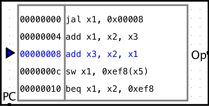
RISC-V Program ROM.
A 32-bit wide byte-addressed ROM, with built-in RISC-V assembler. Use the
attributes panel to load a RISC-V assembly file into the ROM. The
PC input specifies the address of the current instruction,
and must be a multiple of 4. The output is the 32-bit machine code
instruction at the PC address, or an error if the PC is invalid.
Reading addresses outside the range of code supplied by the assembly
file will cause the ROM to output zero, which happens to encode a no-op
in RISC-V. The assembly language is in the format described below. When
we say that the instruction ROM is byte-addressed memory, we mean that
the instruction ROM takes an address A as input, advances A bytes into
its memory (remember, 1 byte = 8 bits), and outputs the 32-bit
instruction that starts at the resulting position. 32 bits is 4 bytes,
which is why the PC normally increments by 4 every cycle: it's simply
going to the next instruction.
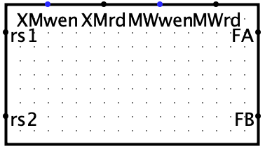
Bypass Black Box.
This component takes in the first source register rs1 and the second source resigster Forwarding is done according to the following logic:
if (MEM/WB.RegWrite and (MEM/WB.RegisterRd != 0) and not (EX/MEM.RegWrite and (EX/MEM.RegisterRd != 0) and (EX/MEM.RegisterRd == ID/EX.RegisterRs1)) and (MEM/WB.RegisterRd == ID/EX.RegisterRs1)) ForwardA = 01
if (MEM/WB.RegWrite and (MEM/WB.RegisterRd != 0) and not (EX/MEM.RegWrite and (EX/MEM.RegisterRd != 0) and (EX/MEM.RegisterRd == ID/EX.RegisterRs2)) and (MEM/WB.RegisterRd == ID/EX.RegisterRs2)) ForwardB = 01
Inputs and Ouputs
- rs1 - First source register (in decode)
- rs2 - Second source register (in decode)
- XMwen - Execute/Memory pipeline register destination write-enable
- XMrd- Execute/Memory pipeline register destination address
- MWwen - Memory/Writeback pipeline register destination write-enable
- MWrd - Memeory/Writeback pipeline register destination address
- FA - Forward A
- FB - Forward B
Decode Black Box.
Inputs and Outputs
- Inst - Takes in the 32-bit instruction
- rs1 - First source register
- rs2 - Seocnd source register
- rd - Destination register
- ALUOp - Op code for the ALU. only for Table A
- Imm - The immediate value of the instruction. Right aligned such that the least
significant n bits are the immediate, where n is the length of the immediate for that particular instruction - UseImm - Boolean that is 1 if the instruction type has an immediate; 0 otherwise.
- ADD, ADDI, ... , BGEU - one-hot encoding for the instruction
For any table-b instruction, behavior is undefined for ALUOp, UseImm, and Imm.
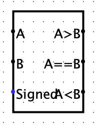
Comparator Black Box.
Inputs and Outputs
- A - Input A
- B - Input B
- Signed - Whether to do a signed comparison
- A > B - 1 if A > B; 0 otherwise
- A = B - 1 if A == B; 0 otherwise
- A < B - 1 if A < B; 0 otherwise
ALU.
Computes a result as follows. You do not need to test the provided ALU, and can assume it will work exactly as specified.
| Op | name | C | V |
|---|---|---|---|
| 101x | shift left logical | C = A << Sa | V = 0 |
| 100x | add | C = A + B | V = overflow |
| 1110 | shift right logical | C = A >>> Sa | V = 0 |
| 1111 | shift right arithmetic | C = A >> Sa | V = 0 |
| 110x | subtract | C = A - B | V = overflow |
| 0011 | and | C = A & B | V = 0 |
| 0001 | or | C = A | B | V = 0 |
| 0111 | xor | C = A ^ B | V = 0 |
| 0101 | nor | C = ~(A | B) | V = 0 |
| 0010 | eq | C = (A == B) ? 000...0001 : 000...0000 | V = 0 |
| 0000 | ne | C = (A != B) ? 000...0001 : 000...0000 | V = 0 |
| 0110 | gt | C = (A > 0) ? 000...0001 : 000...0000 | V = 0 |
| 0100 | le | C = (A ≤ 0) ? 000...0001 : 000...0000 | V = 0 |
Note a small difference between this ALU and the one built in Project 1: the three shift operators shift A instead of B.
Incrementer.
An adjustable-width incrementer. Takes its input A on the
left and outputs A+1 on the right. You must use this
increment for your Program Counter (PC); you cannot build your own
adder to increment the PC. Also, only ONE incrementer is allowed.
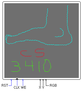
LCD Video.
If WE is high on the rising edge of
CLK, writes a pixel on the LCD screen at the location
given by the 7-bit unsigned X and Y
coordinates. The pixel color is specified by 16-bit RGB
input (in 5-5-5 format). The RST input resets the LCD
screen. With some cleverness, you can redirect memory writes to this
device to let your program draw on the LCD screen. Logisim also comes
with some interesting input and output devices which can be used
similarly.
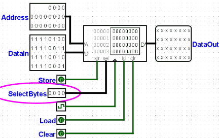
RAM.
Inputs and Outputs
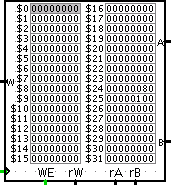
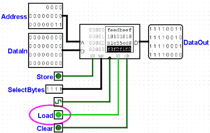
Ais the word-address. Each line in the RAM component is a word (four bytes) in memory, and has a unique address. As in the example figure to the right,A= 0x00002 refers to slot 00002 in the RAM component, which contains a full word. However, for a given address in RAM, if you want to retrieve a specific byte or halfword in the address, you need to use the selector bits (described below). By default, the component's address width is 20 bits (which means that, by default, it can store 2^20 words = 4 * 2^20 bytes = 4MB).Dcontains the data to be stored in RAM. Depending on howselis set, only certain bytes withinDwill be written.stris the store bit. You can think of it as Write Enable. When str = 1, RAM will write the value onDto addressAaccording to the sel bits.selis for the selector bits. As mentioned above, bits 0..7 ofDcorrespond tosel= 0001, bits 8..15 correspond tosel= 0010, bits 16..23 to 0100, and bits 24..31 to 1000.selaccepts other combinations like 1100 (to grab the upper halfword), 1111 (to grab the full word), or even something wacky like 1010.ldis the load bit. Data OutDalways sets floating values (X's) along the wire unless the appropriate selector bits are set and ld = 1.clrclears all of RAM whenever it is 1.
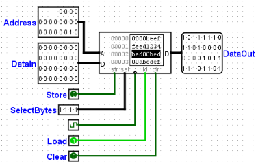
Using the Byte Selector
As previously mentioned, address A gets us to the word in memory. However, we need
to use sel to determine which bytes in the word we want to write to or read from.
The Byte selector is 4 bits, and you can think of each bit as a read/write enable for each
of the four bytes in the word.
Specifically, bit 0 of sel enables the first byte from the right in the RAM component.
When writing to RAM, bits 0 to 7 of DataIn are written to this byte, and when reading from RAM,
the byte's value gets read out to bits 0 to 7 of DataOut. Bit 1 of sel enables the
second byte from the right, and corresponds with bits 8 to 15 of DataIn and DataOut. Bit 2 enables
the third byte from the right and corresponds with bits 16 to 23, and bit 3 enables the fourth byte,
and corresponds with bits 24 to 31.
Storing
Writing into the RAM component requires that the str bit is set to 1.
In the example to the right, DataIn is set so that a hex value 0xf1 is in the bottom line (bits 7..0),
0xf2 is in the second line (bits 15..8), 0xf3 is in the third line (bits 23..16), and 0xf4 is
in the top line (bits 24..31). The gif demonstrates how to write different bytes or
halfwords to the RAM.
When you want to write a byte to a location in RAM, pay attention that you place the
byte-values in DataIn correctly with selector bits. In the example above, if you wanted to
write 0xf1 to left-most byte, you would need to put 0xf1 in bits 24..31 in DataIn and
set sel = 1000.
Loading
Reading from the RAM component requires that the ld bit is set to 1.
Loading is a bit more straightforward. Just be sure that when you are reading a byte from memory
that you retrieve the byte from the right bits on DataOut. For example, if you were only selecting
with sel = 0100, then you'd have to make sure that, when you're splitting DataOut, that you
isolate the correct byte (bits 23..16).
A Note on Implementing Byte Addressed Memory
All the addresses that we deal with in the instruction set are expressed in terms of byte addresses.
This means that address 0x0000 refers to the first byte in memory, and 0x0001 the second byte, and so on.
Since every word has four bytes (in other words, since every four bytes is a new word), then 0x0000 still refers to the first word,
but the second word is at address 0x0004.
It is key that you understand that the RAM is word addressed. It is an error to pass the raw byte-address into the A input.