Group Project 3 - Fully Pipelined MIPS
CS 3410 Spring 2018
Work-in-progress Circuit Due: 11:59pm, Thursday, March 22, 2018
Feedback will be given by Sunday, March 25, 2018
Final MIPS Circuit Due: 11:59pm, Thursday, March 29, 2018
Circuit Naming: Your top-level circuit must be named either "MIPS" or "MIPS32" (case-sensitive).
Late Policy: Slip days can be used for the final submission but not for work-in-progress circuit. If a slip day is used, it will be used for both partners.
You must work with the same partner from project 2. You can change partners for the later projects.
Warning: Read the ENTIRE writeup before you begin. This is cumulative. Both Table A and Table B instructions are required.
Overview
In this project you will extend and complete the processor design you started in project 2. Your basic execution
loop from the previous assignment should contain most of the major components, with the exception of RAM for the
load/store instructions. For this project we will use a split-memory "Harvard" architecture design: The Program ROM
will store a read-only copy of the instructions, and a separate RAM will be used to store data for the program's
execution. You will now implement all the other instructions mentioned in the last project project, including
load/stores, jumps and branches.
You should reuse most or all of your work from project 2. This means updating the circuit to handle the new
instructions, revising the documentation to discuss any changes or addition to the datapath and control logic, and
expanding your test program. This includes, of course, fixing anything that was broken or incomplete from project 2
(ask the staff for help if needed — we will not be posting a solution, but neither do we want to penalize you
twice for mistakes in project 2).
Important: Consult the MIPS Handbook and make sure that all
aspects of each of the instructions is implemented exactly as specified in the handbook, except where noted
here.
Academic Integrity As one of the most widely studied architectures, MIPS has a wealth of information
available on the web and in textbooks. You may consult any of the MIPS architecture documentation available to you in
order to learn about the instruction set, what each instruction does, etc. But we expect your design to be entirely
your own. If you are unsure if it is okay to borrow from some other source, just ask the TAs, and give credit in your
final writeup. If you are unsure about asking the TAs, then it is probably not okay. Plagiarism in any form will not
be tolerated.
What to Submit
Note the different due dates
By Thursday March 22, 2018
- Submit a work-in-progress version of your MIPS circuit on CMS.
- Submit a README file stating what has and has not been implemented.
By Thursday, March 29, 2018
- A single Logisim project file containing your processor and all needed subcomponents.
- A PDF file documenting your processor, including a processor block diagram and description of control logic.
- A text file containing your well-commented MIPS assembly test program.
- A separate file for each of your iterative, recursive, and memoized Fibonacci implementations.
- A git commit history obtained using the command
git log on your repository.
Work-in-Progress Circuit
After receiving feedback on your mini-MIPS circuit from the previous
project you will be required to submit a fixed, work-in-progress
version.
The WIP circuit needs to address and fix all of the errors you had from
project 2, and should not have any extra functionality beyond what was previously
required (i.e all Table B instructions should still be NOPs). We expect the
work-in-progress circuit to work perfectly on project 2 functionalities.
Your submitted work-in-progress circuit should be functional; i.e NO red
wires, NO undefined outputs. Your WIP circuit will be tested on the same
tests from project 2.
What to Implement
Implement all of the instructions in Table B. You should have already decoded all these instructions in project 2.
You may have to add additional decoding logic for any new control signals you introduce, as for the memory stage and
for the PC update.
| Table B |
| Jumps (with one delay slot) |
J, JR, JAL, JALR |
| Branches (with one delay slot) |
BEQ, BNE, BLEZ, BGTZ, BLTZ, BGEZ |
| Memory Load/Store (little endian, with pipeline stall if needed) |
LW, LB, LBU, SW, SB |
Our testing programs will include a mixture of all the instructions from projects 2 and 3, so you must ensure that
the instructions from project 2 are correctly implemented as well.
Deviation from the MIPS standard: You can ignore any MIPS instruction or feature not mentioned in this
document, such as traps, exceptions, and system calls. You can also assume that your processor will never encounter
anything but legal instructions from Tables A and B.
Refer to the MIPS Manual, Volume 2, linked on the course web site for
a full specification of what each of these operations does. Except where noted in here, the MIPS manual is the
authoritative specification for this project: information you find elsewhere (e.g. Wikipedia or the book) doesn't
count if it contradicts the MIPS manual.
One important note: JALR and the implicit $31
The MIPS manual lists two forms of the JALR instruction. This is misleading. There is only one binary encoding for
the JALR instruction, and it is the version that takes two register arguments: JALR rd, rs. This is the
only one you have to implement. The alternate version of JALR, with rd omitted, is just an assembler
pseudo-instruction: whenever you write JALR rs, the assembler converts this to JALR $31, rs before it
encodes it in binary.
Delay slot. You must properly implement the branch/jump delay slot, so that the instruction immediately
following a branch or jump is always executed, and any relative addresses or significant bits for the PC update are
based on the that address and not the address of the jump instruction itself.
Memory load hazard. Memory operations should not have delay slot, but instead use stalling to avoid hazards.
That is, you should introduce a bubble in the pipeline after a memory operation, but only if a hazard is detected.
RAM. The "CS3410 Components" library in the most recent version of Logisim includes a MIPS
RAM component for your memory stage (see the description below). Logisim does not support RAM components large
enough to cover a full 32-bit (4GB) address space. The largest RAM component contains 64MB of data using 24-bit-wide
word-addresses. Our tests will rely on memory addresses in the lowest 1MB of the address space, so your your processor
should contain at least 1MB of RAM placed at the lowest addresses. That is, reads and writes to byte-addresses
in the range 0x00000000 to 0x000fffff should work as expected.
Important: Writes to addresses that not backed by any RAM should
have no effect, and the address space should not "wrap around" after 1MB.
For the adventurous. Instead of having a single RAM component backing the low part of the address space, you
can add multiple RAM components to cover various convenient pieces of the address space. For instance, to support the
conventional MIPS program layout, put a second RAM to cover a few MB of address space near addresses 0x10000000 for
program data, and a third RAM to cover addresses just under 0x80000000 for the stack. Or you can redirect reads and
writes at certain addresses to some of Logisim's input/output devices. It is actually fairly trivial to make writes at
addresses just above 0x80000000 write coordinate and color pixel data to an LCD screen component or ASCII characters
to a TTY component. Similarly you can make reads at some designated unused address read from a Logisim Keyboard,
Joystick, or other input component. Bonus points if you can code pong to go with an LCD.
Restrictions and Naming Conventions
As in project 2, build your MIPS processor as a single Logisim circuit
file. Continue to use the components from the "CS3410 Components" library that
we provided.
Do not import circuits from other Logisim files.
Your top-level circuit must be named either "MIPS" or "MIPS32"
(case-sensitive).
Your processor should have only one instance of each of these
components: Register File, MIPS Program ROM, and ALU.
The register file must be visible either in the toplevel circuit or one level
down in a subcircuit. Do not nest the register file in two or more levels down!
The restriction on incrementers and comparators has been relaxed since
Project 2:
- You may now use more than one incrementer, although incrementing PC by 4
should still be done with one incrementer rather than four.
- You may use as many comparators as you like, however you will still be
penalized for usages that are extremely inefficient.
You can additionally use any of the components that come with Logisim,
such as a Register for the PC, multiplexers, and so on.
Testing
Write a test program in MIPS assembly that fully tests all of the
features from both project 2 and project 3. As before, the program
should be well commented, indicating what it is doing and what results
should be expected when running the program, so that the course staff
is convinced of the correctness of your processor.
We would also like you to test your program on a complex
computation. As such, you should implement the
Fibonacci sequence in iterative, recursive, and
memoized styles.
Fibonacci
The Fibonacci sequence is defined as follows: start
with 0, 1; for the code you are implementing, the zeroth Fibonacci number is
defined to be 0, and the first Fibonacci number is defined to be 1. To
obtain subsequent numbers in the sequence, we take the sum of the previous
two numbers in the sequence. Thus, the second number in the seqeuence is
0 + 1 = 1, and the third number in the sequence is 1 + 1
= 2. The function you implement will return the nth Fibonacci number,
where the value n is an input to your function.
There are several ways to compute the Fibonacci sequence. You will
implement all three of the methods below (please do not submit
MIPS code with any form of main function).
Iterative Fibonacci: An efficient approach for computing the
answer for just a single index in the sequence.
    int i_fibonacci(int n) {
        int f1 = 0;
        int f2 = 1;
        int fi;

        if (n == 0) {
          return 0;
        }

        if (n == 1) {
          return 1;
        }

        for (int i = 2; i <= n; i++) {
            fi = f1 + f2;
            f1 = f2;
            f2 = fi;
        }
        return fi;
    }
Recursive Fibonacci: Simple but inefficient. Logisim will be too slow to use this version except when the
index is small.
    int r_fibonacci(int n) {
        if (n == 0) {
            return 0;
        }
        else if (n == 1) {
            return 1;
        }
        return r_fibonacci(n-2) + r_fibonacci(n-1);
    }
Memoization Fibonacci: For computing the answer for more
than one index, it makes sense to remember previously computed
answers since answers for larger indices require answers for smaller
indices. So if fibonacci(40) and fibonacci(39) has
already been computed, then it is easy to
compute fibonacci(41). This memoization version is essentially
the same as the recursive version but takes two extra arguments: an
array log_array of previously computed answers (should be initialized
to all zeros), and the number of entries size in the array.
Note: the memoized Fibonacci does not allocate or initialize the
array. It assumes that the function calling m_fibonacci has already
created an array of size size and initialized every entry to zero.
    int m_fibonacci(int n, int log_array[], int size) {
        if (n < size && log_array[n] != 0) { // non-zero means we already computed this
            return log_array[n];
        }
        if (n == 0) {
            return 0;
        }
        else if (n == 1) {
            return 1;
        }
        int answer = m_fibonacci(n-2, log_array, size) + m_fibonacci(n-1, log_array, size);
        if (n < size) {
            log_array[n] = answer; // save answer for reuse later
        }
        return answer;
    }
Implement these three versions of the Fibonacci function using MIPS
assembly code. They must all work on your processor in Logisim, though
you will have to be careful when testing to select indices whose Fibonacci
number can be computed in a reasonable time.
Testing and input for Fibonacci functions
Your Fibonacci functions are just that: functions. They should get
their inputs from the argument registers ($a0,
$a1, etc.) and they should return their results via register
$v0. To test the functions, you will nead to create a "main"
program which initializes the stack (by setting $sp and
$fp to something reasonable and usable), puts some input in the
argument registers, then calls the function via JAL. The
Fibonacci functions never make system calls or any other function calls that
could possibly read input from the user. Your main program could if you
managed to wire up a keyboard though.
Documentation
Document your design in the same fashion as project 2. Be sure to revise your block diagram to show any new
components, and to revise your descriptions of control and instruction decoding logic to account for any changes or
additions.
Help and Hints
MIPS calling conventions and program layout. The three versions of
Fibonacci must be implemented as functions: they should take arguments and
return results in registers (or on the stack), and use a call stack
for recursive invocations. For this project, you are
required to follow MIPS calling convention (as covered in class)
precisely. You are expected to create these functions
manually.
cs3410 Component Library Guide
The "CS3410 Components" library will only appear if you are using the most recent version of Logisim, downloaded from the course website. Please ensure that you are using the correct version. If so, you should have a folder in your sidebar containing the CS 3410 Components.
Using MIPS RAM as byte addressed and little endian RAM
For an in-depth guide of the RAM component: Click here
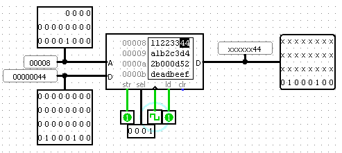
Here is a screenshot as I am writing the byte value 0x44 into byte address 32. Since the RAM is word addressed, this
byte gets written to one of the four bytes at word address 32/4 = 8; you can see the A input to the RAM is 8. Since I
want little-endian behavior, address 32 corresponds to the little end of the word (address 35 would be the big end of
the same word, where 0x11 is stored); you can see the selector input is set to activate only the little end of the word. I
am also reading at the same time, so you can see the 0x44 being read out on the litle end of the D output. If I were to
activate all of the selectors, the RAM would output 0x11223344, which is the word stored at word address 8, i.e. byte
address 4 * 8 = 32, which contains bytes 32 through 35.
Here is another screenshot as I am writing the byte value 0x2b into byte address 43. Since the ram is word addressed, this
byte gets written to one of the bytes at word address 43/4 = 10; you can see the A input to the RAM is 0xa = 10. Since I
want little-endian behavior, address 43 corresponds to the big end of the word (address 40 would be the little end of
the same word, where 0x52 is stored); you can see the selector input is set to activate only the big end of the word. I
am also reading at the same time, so you can see the 0x2b being read out on the big end of the D output. If I were to
activate all of the selectors, the RAM would output 0x2b000d52, which is the word stored at word address 0xa = 10, i.e. byte
address 4 * 10 = 40, which contains bytes 40 through 43.

For writing byte 0xbb, depending on the address, I might want to put it at the big end, little end, or somewhere in the
middle. Similarly for reading a byte, depending on the address, I might want to grab the bytes from the big end, little
end, or somewhere in the middle. Hint: For writing, just direct the desired byte to all four positions then
activate writing for just the one you want. For reading, you will need to select between the four possible positions
where the byte might appear on the RAM's D output.
On the other hand, reading and writing whole words is trivial. The RAM is 32 bits wide, so just send the whole
32-bits to the memory, and read the whole 32-bits back to the CPU. You could try to be clever by swapping the
order of each word's four bytes when writing to RAM, and un-swapping them when reading from RAM. This, however, would be
entirely pointless. Can you tell why? Try it to see if it makes it any easier to read and write bytes.
It is critical that your circuit adheres to the
CS3410 Logisim Design Guidelines to avoid losing points!
MIPS (subset) Assembly Syntax
The MIPS Program ROM component has a built-in assembler that understands all of the instructions you will
implement. The syntax is standard MIPS syntax. Labels are case sensitive, everything else ignores case. Anything
following a pound ('#') is a comment. In this project, you will only use a few of the instructions listed
here.
The instruction syntax is the same as given in the MIPS standard (and different from the output of gcc and
many other tools). Registers are written as $0, $1, ..., $31, and the destination register
goes on the left, followed by source registers and immediate values on the right. Most integer arguments (immediates,
shift amounts, jump targets) can be specified in hex (i.e. 0x12ab), in decimal (i.e. 1234 or -1234), a label, or the
special constant PC. The assembler will replace PC with the address of the instruction itself. Most
constants have some restrictions: jump destinations must have the same upper 4 bits as the PC+4, and must be
a multiple of 4; branch destinations must be a multiple of 4 and fit in a signed 18 bit immediate; etc. As a special case, when a branch
target is specified symbolically as a label, the assembler will automatically subtract the current PC value to obtain
a signed offset.
By default, the first instruction will be placed at address 0, and subsequent instructions are placed at at
addresses 4, 8, 12, etc.
Assembler directives. The Program ROM assembler understands two standard MIPS assembler directives, .text and
.word, both of which take integer (hex or decimal) arguments. For example, .text 0x50000000 will
direct the assembler to place subsequent instructions starting at address 0x50000000. And .word 0x24030005
directs the assembler to use the value 0x24030005 as the next machine instruction, which happens to be the machine
code for ADDIU $3, $0, 5.
Symbolic register names. The assembler built into the MIPS Program ROM accepts
standard MIPS register names: $zero, $at, $v0, $v1, $a0 - $a4, $s0 - $s7, $t0 - $t9, $k0, $k1, $sp, $gp, $fp, and $ra.
Some examples of instructions are:
| Immediate Arithmetic |
ADDIU $12, $0, PC |
| Register Arithmetic |
ADDU $13, $0, $20 |
| Immediate Load |
LUI $14, 0x123 |
| Shifts |
SLL $13, $13, 2
SLLV $15, $14, $3
|
| Jumps |
J 0x24
J my_label
JR $5
JALR $31, $5
JALR $5
|
| Branches |
BEQ $5, $6, -12
BEQ $5, $6, my_loop_top
BLEZ $9, 16
BLEZ $9, my_loop_done
|
| Memory Load/Store |
LW $12, -4($30)
SW $12, 0($30)
|
MIPS (subset) Opcode Summary (from the MIPS Handbook)
Items in white are required for this project. Make sure to implement all of them. The grayed out items are not implemented, and you do not need to worry about them.
Table 1: MIPS32 Encoding of the Opcode Field
| opcode
|
bits
28..26 → |
|
| ↓ bits 31..29 |
0 |
1 |
2 |
3 |
4 |
5 |
6 |
7 |
| 000 |
001 |
010 |
011 |
100 |
101 |
110 |
111 |
| 0 |
000 |
SPECIAL δ |
REGIMM δ |
J |
JAL |
BEQ |
BNE |
BLEZ |
BGTZ |
| 1 |
001 |
ADDI |
ADDIU |
SLTI |
SLTIU |
ANDI |
ORI |
XORI |
LUI |
| 2 |
010 |
COP0 δ |
COP1 δ |
COP2 θδ |
COP3 θδ |
BEQL φ |
BNEL φ |
BLEZL φ |
BGTZL Φ |
| 3 |
011 |
β |
β |
β |
β |
SPECIAL2 δ |
JALX ε |
ε |
* |
| 4 |
100 |
LB |
LH |
LWL |
LW |
LBU |
LHU |
LWR |
β |
| 5 |
101 |
SB |
SH |
SWL |
SW |
β |
β |
SWR |
CACHE |
| 6 |
110 |
LL |
LWC1 |
LWC2 θ |
PREF |
β |
LDC1 |
LDC2 θ |
β |
| 7 |
111 |
SC |
SWC1 |
SWC2 θ |
* |
β |
SDC1 |
SDC2 θ |
β |
Table 2: MIPS32 SPECIAL Opcode Encoding of the
Function Field
| function
|
bits
2..0 → |
|
| ↓ bits 5..3 |
0 |
1 |
2 |
3 |
4 |
5 |
6 |
7 |
| 000 |
001 |
010 |
011 |
100 |
101 |
110 |
111 |
| 0 |
000 |
SLL |
MOVCI δ |
SRL |
SRA |
SLLV |
* |
SRLV |
SRAV |
| 1 |
001 |
JR |
JALR |
MOVZ |
MOVN |
SYSCALL |
BREAK |
* |
SYNC |
| 2 |
010 |
MFHI |
MTHI |
MFLO |
MTLO |
β |
* |
β |
β |
| 3 |
011 |
MULT |
MULTU |
DIV |
DIVU |
β |
β |
β |
β |
| 4 |
100 |
ADD |
ADDU |
SUB |
SUBU |
AND |
OR |
XOR |
NOR |
| 5 |
101 |
* |
* |
SLT |
SLTU |
β |
β |
β |
β |
| 6 |
110 |
TGE |
TGEU |
TLT |
TLTU |
TEQ |
* |
TNE |
* |
| 7 |
111 |
β |
* |
β |
β |
β |
* |
β |
β |
Table 3: MIPS32 SPECIAL REGIMM Encoding of the
rt Field
| rt
|
bits
18..16 → |
|
| ↓ bits 20..19 |
0 |
1 |
2 |
3 |
4 |
5 |
6 |
7 |
| 000 |
001 |
010 |
011 |
100 |
101 |
110 |
111 |
| 0 |
00 |
BLTZ |
BGEZ |
BLTZL |
BGEZL |
* |
* |
* |
* |
| 1 |
01 |
TGEI |
TGEIU |
TLTI |
TLTIU |
TEQI |
* |
TNEI |
* |
| 2 |
10 |
BLTZAL |
BGETAL |
BLTZALL |
BGETALL |
* |
* |
* |
* |
| 3 |
11 |
* |
* |
* |
* |
* |
* |
* |
* |