Remember that we expect you to work in groups of two for all programming assignments.
Overview In the first three programming assignments you will design and implement a subset of the MIPS32 architecture in Logisim, a software logic simulator. By the end of this assignment we will implement a 32-bit pipelined version of the MIPS architecture. We will ignore more advanced features such as the MIPS coprocessor instructions and traps/exceptions for these three programming asssignments. Read this document entirely before implementing your assignment.
Academic Integrity As one of the most widely studied architectures, MIPS has a wealth of information available on the web and in textbooks. You may consult any of the MIPS architecture documentation available to you in order to learn about the instruction set, what each instruction does, etc. But we expect your design to be entirely your own. If you are unsure if it is okay to borrow from some other source, just ask the TAs, and give credit in your final writeup. If you are unsure about asking the TAs, then it is probably not okay. Plagiarism in any form will not be tolerated.
Programming Assignment 3: Pipelined MIPS Processor
In this project you will complete the design of your MIPS processor by adding most of the remaining MIPS instructions. Your basic execution loop from the previous project should contain most of the major components, with the exception of RAM for the load/store instructions. For this project, we will use a split-memory design: The Program ROM will store a read-only copy of the instructions, and a separate Logisim RAM will be used to store data for the program's execution.
This version of your processor will be pipelined according to the MIPS standard, which specifies four stages:
- Fetch
- Arithmetic
- Memory access
- Write back
Refer to the MIPS standard, volume I, section 2.6.1 for details. Note that the book describes a five-stage pipeline, which is not what you will be implementing; stick to the standard where there are differences.
It is now required that you correctly implement the delay slot, which means that the instruction immediately following a jump is always executed, and any relative addresses or significant bits are based on that address and not the address of the jump instruction itself.
Additionally, your processor must handle the following instructions:
| Jumps (with a delay slot) NEW | J, JR, JAL, JALR |
| Branches (with a delay slot) NEW | BEQ, BNE, BLEZ, BGTZ |
| Memory Load/Store NEW | LW, SW |
| Immediate Load NEW | LUI |
| Immediate arithmetic | ADDIU, ANDI, ORI, XORI |
| Register arithmetic | ADDU, SUBU, AND, OR, XOR, NOR |
| Shifts (constant and variable) NEW | SLL, SRL, SRA, SLLV, SRLV, SRAV |
Write a test program that fully tests all of the features you have implemented in this project. This is a critical step, and you should spend a fair amount of time developing a comprehensive set of test programs that exercise all of the different parts of your processor.
Components you will need The cs316 library contains a "Register File," a triple-ported (dual read, single write) 32-bit wide by 32-registers deep register file; a "MIPS Program ROM," a program memory module capable of loading a MIPS assembly language file directly into its memory; a "Mips ALU," an ALU module encapsulating a working solution to PA1; and an "Incrementer (General)" for you to use to increment the PC. More detailed descriptions of these components can be found below.
For this assignment, do not use your ALU from PA1. Instead,
you are required to use the "Mips ALU" component included in the cs316
library. We are also requiring that you use the "Incrementer (General)"
to increment the PC. (Note that the incrementer only computes +1,
whereas the PC increments by 4.)
By using these components, you will reduce your chances of triggering a
bug in Logisim's simulator and make it easier for us to grade your
circuit.
Logisim's memory library contains registers you can use for your program counter and pipeline connections, as well as a RAM component for storing memory.
What to submit Submit a single Logisim project file containing your processor and a text file containing a MIPS assembly test program of your choice. The test program should exercise the instructions and features of the processor enough to convince the staff of its correctness. Please comment your program, indicating what it is doing and what results should be expected when running the program. If you want, you can submit a brief writeup.
Help and Hints Ask the TAs and consultants for help. You can contact us through the course staff mailing list or the class newsgroup. We also expect to see most students in office hours during the course of the project. Extra hours will be scheduled as needed.
If you suspect a bug in Logisim or the cs316 library, ask the course staff for help. There is a known bug having to do with bus splitters when the simulation is running. It is best to turn the simulator off when editing the wire ordering on a bus splittter. This does not cause any data loss, but you might have to restart Logisim.
Deviation from the MIPS standard You can ignore any MIPS instruction or feature not mentioned in this document, and can assume that your processor will never encounter anything but legal instructions from the list above. In addition:
- Assume all jumps will be word aligned and to valid ROM addresses.
- Assume traps or exceptions will not occur (i.e., do not implement them).
- Use a split-memory design with separate RAM for memory and ROM for program code.
Logisim and cs316 Library Guide
Logisim and the cs316 library are available on the course homepage.
|
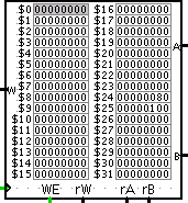
Register File A 32-bit wide by 32-registers deep register file. Register $0 is hard-wired to zero at all times, and writes to $0 are ignored. Inputs rA and rB are used to select register values to output on the A and B outputs. On the falling edge of the clock, if WE is high, the data value at input W is stored in register rW. |
 |
|
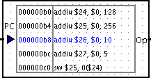
MIPS Program ROM A 32-bit wide byte-addressed ROM, with built-in MIPS assembler. Use the attributes panel to load a MIPS assembly file into the ROM. The PC input specifies the address of the current instruction, and must be a multiple of 4. The output is the 32-bit instruction at the PC address, or zero if the PC has gone past the end of the ROM. Note that zero also happens to encode a no-op in MIPS. The assembly language is in the format described below. |
 |
|
Mips ALU An ALU component encaspulating the solution to PA1. |
 |
|
Incrementer (General) An
adjustable-width incrementer. Takes its input A on the left
and outputs A+1 on the right.
|
|
|
Logisim RAM Configurable to 32-bit
wide word-addressed RAM with up to 12 bits address space (16KB).
Logisim help describes the chip in more detail. Since it is word
addressed, be sure to drop the lowest two bits from the address; as
well as the extra high order bit. Use a tri-state buffer to drive the
bidirectional D pin. The following is a typical circuit. |
|
 |
|
MIPS (subset) Assembly Syntax
Some examples of instructions are:
| Jumps | J 0x24 J my_label JR $31 |
| Branches | BEQ $5, $6, -12 BEQ $5, $6, my_loop_top BLEZ $9, 16 BLEZ $9, my_loop_done |
| Memory Load/Store | LW $12, -4($30) SW $12, 0($30) |
| Immediate Load | LUI $14, 0x123 |
| Immediate Arithmetic | ADDIU $12, $0, PC |
| Register Arithmetic | ADDU $13, $0, $20 |
| Shifts | SLL $13, $13, 2 SLLV $15, $14, $3 |
| Labels | my_loop_top: BNE $5, $6, 16 my_loop_done: |
MIPS (subset) Opcode Summary (from the MIPS Handbook)
NB: Items in white are required for this assignment.
| opcode | bits 28..26 → | ||||||||
| ↓ bits 31..29 | 0 | 1 | 2 | 3 | 4 | 5 | 6 | 7 | |
| 000 | 001 | 010 | 011 | 100 | 101 | 110 | 111 | ||
| 0 | 000 | SPECIAL δ | REGIMM δ | J | JAL | BEQ | BNE | BLEZ | BGTZ |
| 1 | 001 | ADDI | ADDIU | SLTI | SLTIU | ANDI | ORI | XORI | LUI |
| 2 | 010 | COP0 δ | COP1 δ | COP2 θδ | COP3 θδ | BEQL φ | BNEL φ | BLEZL φ | BGTZL Φ |
| 3 | 011 | β | β | β | β | SPECIAL2 δ | JALX ε | ε | * |
| 4 | 100 | LB | LH | LWL | LW | LBU | LHU | LWR | β |
| 5 | 101 | SB | SH | SWL | SW | β | β | SWR | CACHE |
| 6 | 110 | LL | LWC1 | LWC2 θ | PREF | β | LDC1 | LDC2 θ | β |
| 7 | 111 | SC | SWC1 | SWC2 θ | * | β | SDC1 | SDC2 θ | β |
| function | bits 2..0 → | ||||||||
| ↓ bits 5..3 | 0 | 1 | 2 | 3 | 4 | 5 | 6 | 7 | |
| 000 | 001 | 010 | 011 | 100 | 101 | 110 | 111 | ||
| 0 | 000 | SLL | MOVCI δ | SRL | SRA | SLLV | * | SRLV | SRAV |
| 1 | 001 | JR | JALR | MOVZ | MOVN | SYSCALL | BREAK | * | SYNC |
| 2 | 010 | MFHI | MTHI | MFLO | MTLO | β | * | β | β |
| 3 | 011 | MULT | MULTU | DIV | DIVU | β | β | β | β |
| 4 | 100 | ADD | ADDU | SUB | SUBU | AND | OR | XOR | NOR |
| 5 | 101 | * | * | SLT | SLTU | β | β | β | β |
| 6 | 110 | TGE | TGEU | TLT | TLTU | TEQ | * | TNE | * |
| 7 | 111 | β | * | β | β | β | * | β | β |