| ECE/CS 314: Computer Organization Fall 2004 |
| Project 4: MIPS Processor (Part 1: Datapath) |
| Due: November 22, 2004 |
| Basics | |
|
All ECE/CS 314 projects, including this one, are done in groups of exactly two students. Please link up with a partner and submit a single solution. If you do not have a partner yet and cannot find one, use the course newsgroup to find one. Please read this document completely before starting.
|
| Project Goal | |
|
This part of the ECECS314 project has a single goal: to make sure you have thought through your entire pipelined MIPS datapath, including all the control signals and bypass paths, before you write any CAST descriptions. Completing this document should be all the proof you need to convice yourself that your design works. |
| Part 1: Datapath Design Drawing | |
|
The first part of this project is to draw a datapath diagram for your 5-stage
pipelined MIPS processor implementation. The datapath should be capable of
handling all the instructions implemented in your MIPS simulator from Project
2, with the exception of The processor pipeline has the following 5 stages:
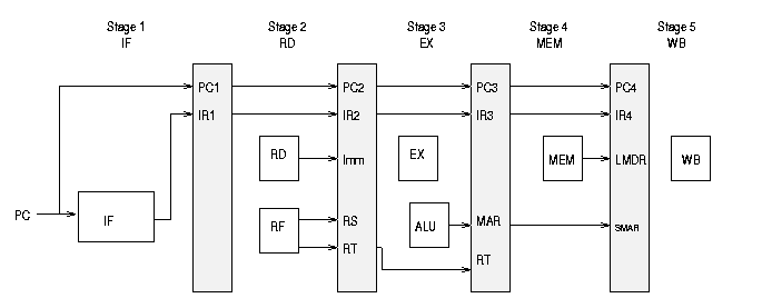
Each pipeline stage has a number of pipeline registers (shown in the figure above) immediately following the stage to save the computed values necessary for the next stage. Assume all pipeline registers are positive edge triggered, as described in lecture, and the PC and register file are negative edge triggered. The figure shows some values you will need to flop from one stage to another. You may flop additional values if you wish. Note: not all data-dependencies are shown in the figure above. The MIPS register file and memory behave as described in the lecture notes. You are to extend this figure to a complete datapath diagram. This will require you to add MUXes (and control signals) to route data as needed to implement all the required instructions, including all necessary bypass paths . In addition to MUXes, your datapath diagram will need some additional parts – for example, an adder to be used in updating the PC, a sign-extension unit for immediate operands, and so forth. You must show all the control signals needed to implement any of the required instructions. However, you do not (yet) need to design the logic required to generate your control signals. That will come later. Your datapath MUST be drawn using Microsoft Visio. Visio is installed in the Phillips 318 and the CSUG labs. To simplify the creation of your datapath diagram, we've created the following visio stencil and template: ececs314 stencil - a group of parts that can be placed in the following template ececs314 template - the starting point for your datapath diagram |
| Part 2: Design Document | |
|
The design document consists of three parts:
Consider the following sequence of MIPS instructions: lw instruction at location 0x110
and ending when the sw instruction at location 0x128 completes.
This document can be either a .pdf, .doc or .txt file . |
| Submitting Your Project | |
|
Both an electronic copy, as well as a hard copy are required. The hard copy is compiled as follow: title page, readme, datapath diagram, and design document. The hard copy can be submitted during the lecture on Tuesday (November 23rd) or can be handed over to any of the TAs during the office hours. The electronic copy must be submitted through CMS by Monday November 22nd at 11:59 pm. Your hard copy must exactly match the electronic copy submitted, an attempt to submit a more complete project in section, as compared to the electronic submission, will be considered cheating (no excuses will be accepted for this). The electronic submission contains the following three files:
|
| List of Instructions | |
|
The complete list of required MIPS instructions is: |